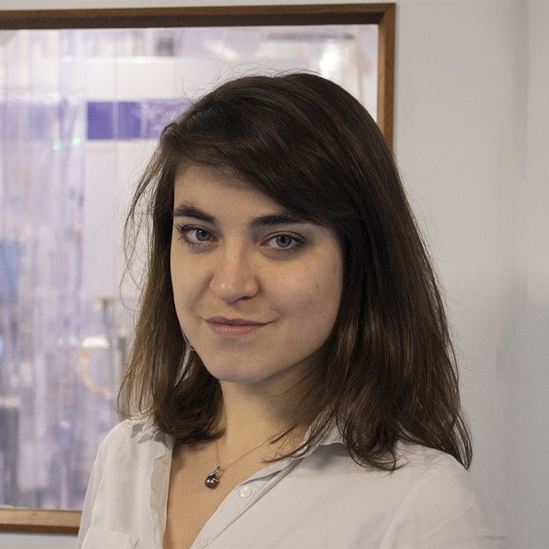
Pauline Alvarez, Oxford Instruments, Atomic Layer Deposition for Quantum Technologies

Zoom Details
Technical Seminar
10:00 am - 11:00 am
https://ucsb.zoom.us/j/94263027041?pwd=S1FGRS93UXJWbDFURnpDb0xlS0VvQT09
Meeting ID: 942 6302 7041 Password: qfSeminar
Career Talk
11:15 am - 12:00 pm
https://ucsb.zoom.us/j/93857794947?pwd=aDBDcDNyR3NGM1pVZ1krcTl3L0Vvdz09
Meeting ID: 938 5779 4947 Password: qfSeminar
Speaker
Pauline Alvarez
Ion Beam & ALD Specialist
Oxford Instruments Plasma Technology
Bio
Pauline Alvarez is an Atomic Layer Deposition and Ion Beam Sputtering Specialist at Oxford Instruments Plasma Technology, for which she has been working for almost 6 years. She first started as a Process Engineer in IBD/IBE (and reactive variants), and then broadened her horizons to Magnetron Sputtering and Atomic Layer processing. She also worked on thin-film characterization techniques notably via her specialization in Nanophysics at INSA Toulouse, France, and experience at Asylum Research, Santa Barbara, investigating advanced imaging techniques. Her current position consists of further understanding of customer applications and requirements in order to develop solutions tailored to the market’s needs. More specifically, she studies the impact of process parameters and thin film properties on the device performance, examining what can be detrimental to it or enable new applications. She focuses on the thriving market of Quantum Technologies, while also looking into Lasers, Infrared sensors, and AR/VR.
Abstract
During this talk, I will be covering the basics of Atomic Layer Deposition and take you on a tour of some exciting applications in Quantum Technologies. You will hear about atomic-scale processing, plasma versus thermal ALD, the benefit of using table bias for superconducting nitrides, and how combining ALD with pre-treatment and clustering technologies could improve device performance. I will also talk you through our latest process developments and feature some examples of how ALD can be used in quantum circuits, including coating Through-Silicon Vias with superconducting nitrides enabling 3D integration and operation at a higher temperature, depositing superconducting NbN on low-loss SiNx waveguides for Single-Photon Detectors, oxide growth for Josephson Junction tunnel barriers and passivation layers for diamond patterning.