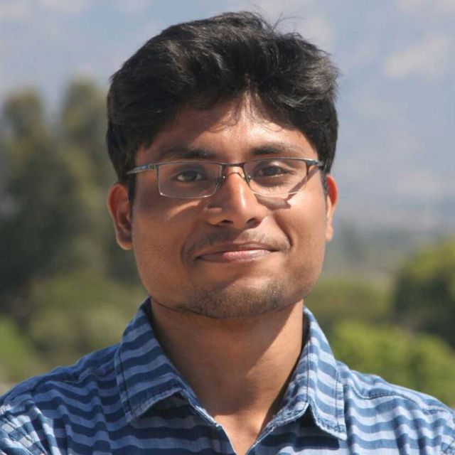
Aranya Goswami (Postdoc at MIT)
Biography
Aranya is from Kolkata,India and pursued his undergraduate degree at the Indian Institute of Technology, Kharagpur- majoring in Electronics and Communication Engineering. During this time, he worked on diverse projects including studying electrical transport on tunnel field effect transistors at IBM SRDC, Bangalore and developing computational models of DNA folding on carbon nanotubes during an internship at EPFL, Switzerland. His undergraduate thesis was in designing analog circuits for neuromorphic computing.
After his undergrad degree, Aranya wanted to work more on the fundamental material side of things and joined the Palmstrøm lab at UC Santa Barbara in Fall 2016 as a PhD student. His work in the past years mainly focused on epitaxial selective area growth of III-V materials using MBE and CBE and subsequently analyzing them in TEM. His current work with the Quantum Foundry will specifically focus on selective area grown semiconductor nanowire systems coupled to superconductors, a system that is being currently explored for topological quantum computation. The aim of his research is to improve the material system by designing and optimizing fabrication and growth processes.