The integration of solid-state single-quantum emitters (SQEs) with chip-scale electronic and photonic circuitry is crucial for advancing quantum information technologies, including linear optical computing, cluster state generation, quantum key distribution, and quantum random number generation. Among the various material systems explored for developing robust single-photon sources, two-dimensional materials (2DMs) are promising due to their distinctive properties. Featuring weak van der Waals forces between their atomically thin layers, 2DMs offer the ability to stack and form unique heterostructures that boast exotic electronic and optical properties distinct from conventional bulk materials. Notably, these emitters exhibit remarkable sensitivity to their local strain environment, serving as a vital tool for interfacing with classical and quantum systems alike.
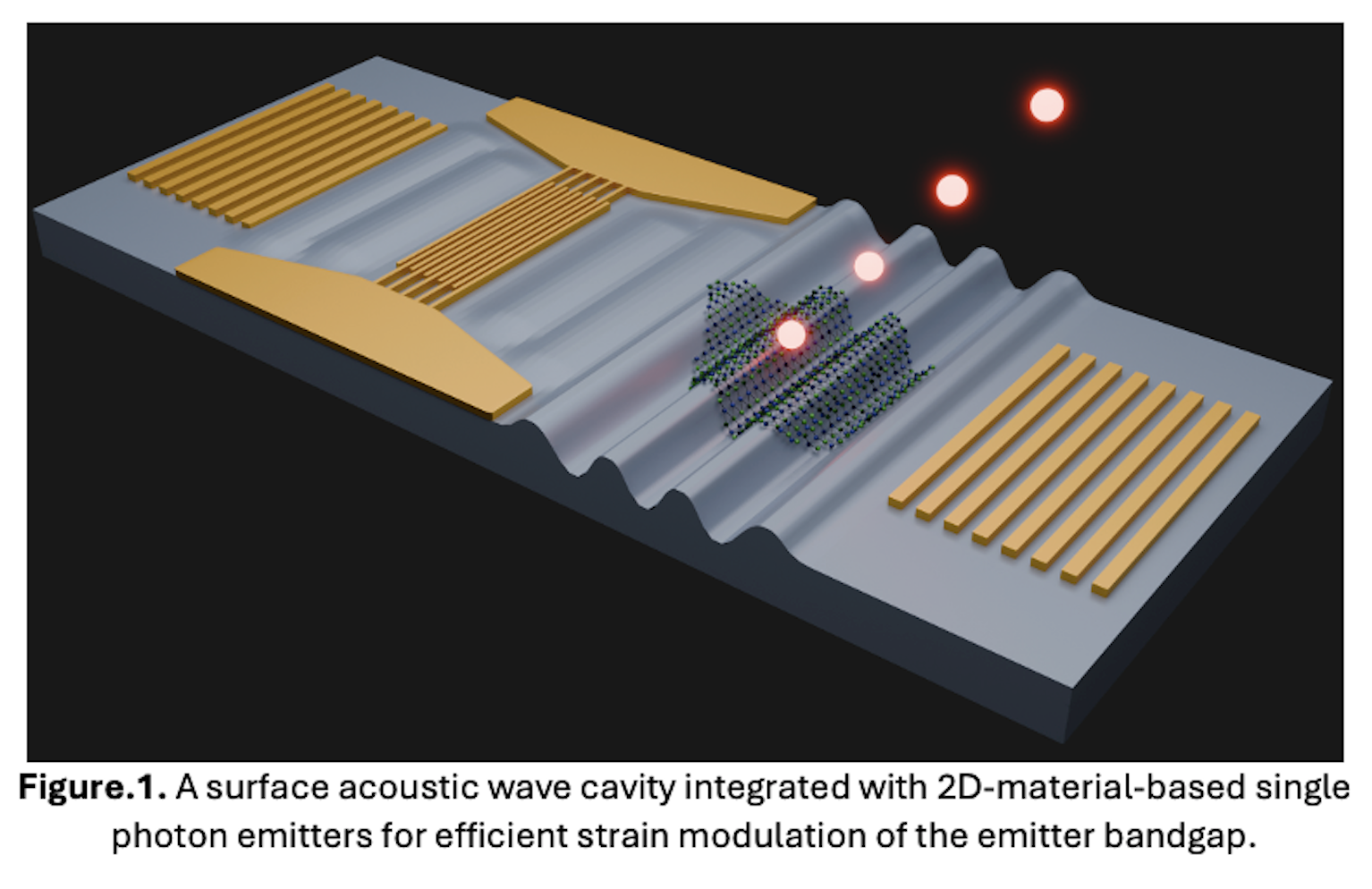
Recent advancements showcase the coupling of emitters in atomically thin h-BN and Tungsten Diselenide (WSe2) with mechanical oscillations in surface acoustic waves (SAWs), offering a pathway for connecting diverse quantum systems1,2. Leveraging the concentrated strain energy density of SAWs at the material surface, researchers demonstrate an optomechanical system where quantum emitters in h-BN and WSe2 are coupled to SAW fields in acoustic resonators. Employing steady-state photoluminescence spectroscopy and time-resolved single-photon counting, the study delves into the time evolution of these emitters as they interact with multiple resonant SAW cavity modes. The results unveil intriguing energy-level splittings consistent with deformation potential coupling, showcasing substantial sensitivity—35 meV/% for WSe2 and 12.5 meV/% for h-BN—underscoring the potential for on-demand entangled-photon-pair generation from 2D materials3.
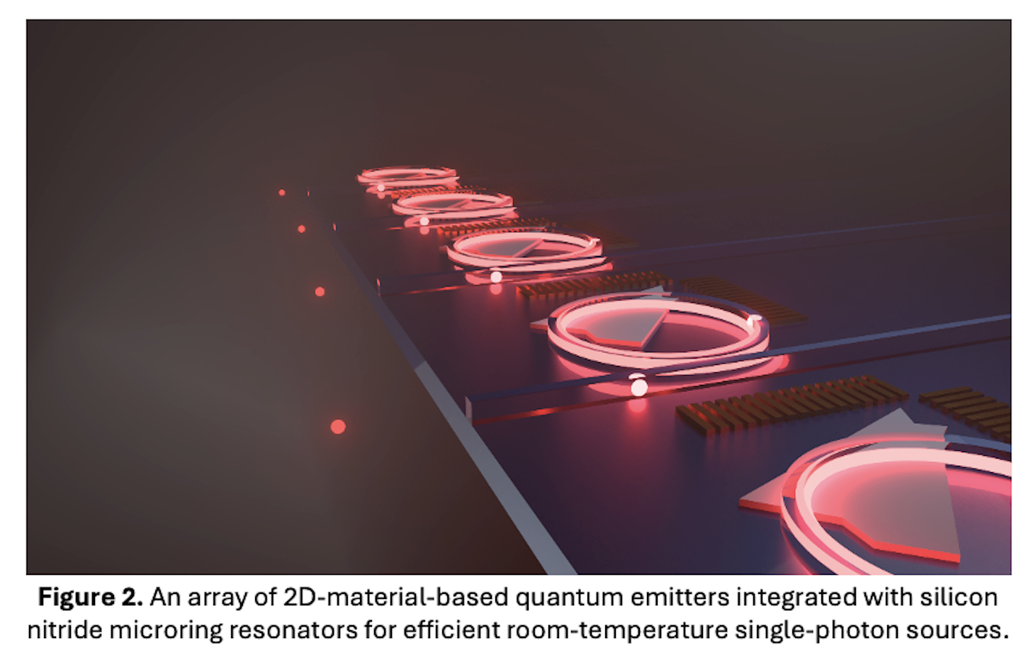
Despite the identification of numerous SQEs capable of high-purity single-photon emission across various materials, integrating them with CMOS-compatible photonics remains a formidable challenge. Overcoming this challenge calls for a hetero-integrated approach, which involves integrating materials by hosting high-quality emitters into the silicon-photonic fabrication flow. Researchers have developed a new approach that created site-controlled arrays of quantum emitters precisely aligned to silicon nitride photonic microresonators, enabling both high-purity and bright single-photon emission on chip4. Their approach utilizes color centers created in hexagonal Boron Nitride. h-BN was chosen due to its wide-bandgap, which enables room-temperature single-photon emission with high photon purity. Emitters can be created and located with better than 100 nm spatial precision, and they can exhibit transform-limited linewidths as narrow as 50 MHz, resulting in near-indistinguishable single-photon emission.
The UCSB team made several advances in photonic integration of h-BN emitters. The first is the growth of high-quality, non-stoichiometric silicon nitride, which eliminates the auto-fluorescence background in stoichiometric Si3N4 films. The second is the process to embed emitters within the photonic waveguiding layer, enabling efficient coupling to a single guided optical mode. The third is the alignment of the emitter position and optical dipole moment with the cavity mode, resulting in >46% on-chip single-photon collection efficiency and > 95% single-photon purity at room temperature. This is the first demonstration of microcavity integration of quantum emitters in two-dimensional material emitters with silicon-based photonics, which improved the on-chip coupling efficiency by an order-of-magnitude over previous demonstrations.
1. Lazić, S., Espinha, A., Pinilla Yanguas, S. et al. Dynamically tuned non-classical light emission from atomic defects in hexagonal boron nitride. Commun Phys 2, 113 (2019), doi: 10.1038/s42005-019-0217-6.
2. M. Choquer et al., "Quantum Control of Optically Active Artificial Atoms With Surface Acoustic Waves," in IEEE Transactions on Quantum Engineering, vol. 3, pp. 1-17, 2022, Art no. 5100217, doi: 10.1109/TQE.2022.3204928.
3. Patel, S., Parto, K., Choquer, M., Lewis, N., Umezawa, S., Hellman, L., Polishchuk, D., & Moody, G. (2024). Surface Acoustic Wave Cavity Optomechanics with Atomically Thin h-BN and WSe_2 Single-Photon Emitters. PRX Quantum, 5, 010330.
4. K. Parto, S. I. Azzam, N. Lewis, S. D. Patel, S. Umezawa, K. Watanabe, T. Taniguchi, and G. Moody. Cavity-Enhanced 2D Material Quantum Emitters Deterministically Integrated with Silicon Nitride Microresonators. Nano Letters 2022 22 (23), 9748-9756
DOI: 10.1021/acs.nanolett.2c03151