Epitaxial Growth and Electronic States of Ultrathin Bi (111) Films on InSb (111)B
(111) Bismuth films hold promise in potential applications in valleytronic and spintronic devices1,2, and 1D-edge transport in the theoretical quantum spin Hall phase3.Yet synthesizing high-quality, large-area (111) ultrathin bismuth films on insulating substrates remains challenging. Here, we demonstrate the growth of large-area (111) Bi films of a single epitaxial domain synthesized on InSb (111)B substrates, with thicknesses ranging from 1 to 200 bilayers. We find evidence of strong film-substrate interactions that allow the epitaxial stabilization of ultrathin bismuth films and lead to inversion symmetry breaking in the bismuth bilayers. Thus far, the topological classification of bismuth as a Z2 topological insulator or a higher order topological insulator has remained elusive, with density functional theory (DFT) predictions and angle-resolved photoemission spectroscopy (ARPES) measurements contradicting each other, claiming Z2 trivial4 and non-trivial5 band topology, respectively. Combining ARPES, scanning tunneling microscopy and spectroscopy (STM and STS), and DFT, we resolve the controversy and show that the bismuth surface states are topologically trivial for both biaxial tensile strained and unstrained films.
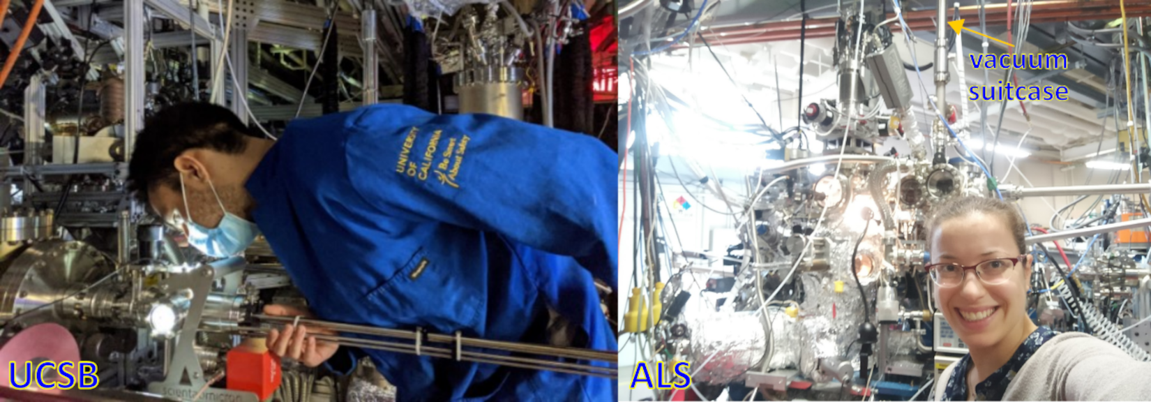
In this work, we have transferred the bismuth films grown via molecular beam epitaxy (MBE) from UCSB in vacuo to the 10.0.1.2 beamline at the Advanced Light Source (ALS) at Lawrence Berkeley National Laboratory. Using an ultrahigh-vacuum (UHV) suitcase, we conducted STM, STS, and ARPES studies for the same films, followed by surface passivation capping at UCSB for ex situ x-ray diffraction (XRD) and magnetotransport measurements. (A) shows the three-fold symmetry of the surface states at the Bi (111) surface Brillouin zone, indicating the films are well-ordered and are in registry with the underlying zinc-blende substrate. STM and XRD measurements confirm the nucleation of conformal single-crystal Bi (111) films. These techniques also shed light on a new ripple-like strain relaxation pathway, unique to van der Waals materials6, and observed for the first time in epitaxially grown films. In (B-C), we present an E-k spectral map along  which show two key features: surface state degeneracy at the
  high symmetry point and quantum-well states dispersion spacing as a function of the film thickness. Inversion symmetry breaking in the bismuth film prevents the hybridization of neighboring surface states at the top and bottom surface, and allows us to rule out bismuth grown on InSb (111)B from being a topological insulator. Ultraviolet photoemission spectroscopy experiments provide evidence of inversion symmetry breaking through signatures of Bi-Sb and Bi-In bonds detected at the film-substrate interface. By tracing the quantum well state energies through a phase accumulation model, we determine that the bismuth layer is subject to a strong confinement potential at the Bi-InSb interface.
References
1 Z. Zhu, A. Collaudin, B. Fauqué, W. Kang, and K. Behnia, Nat. Phys. 8, 89 (2012).
2 A. Takayama, T. Sato, S. Souma, T. Oguchi, and T. Takahashi, Nano Lett. 12, 1776 (2012).
3 S. Murakami, Phys. Rev. Lett. 97, 236805 (2006).
4 I. Aguilera, C. Friedrich, and S. Blügel, Phys. Rev. B 91, 125129 (2015).
5 S. Ito, B. Feng, M. Arita, A. Takayama, R.-Y. Liu, T. Someya, W.-C. Chen, T. Iimori, H. Namatame, M. Taniguchi, C.-M. Cheng, S.-J. Tang, F. Komori, K. Kobayashi, T.-C. Chiang, and I. Matsuda, Phys. Rev. Lett. 117, 236402 (2016).
6 A. Kushima, X. Qian, P. Zhao, S. Zhang, and J. Li, Nano Lett. 15, 1302 (2015).
 path is highlighted, and corresponding E-k cuts are presented in (B-C). (B) ARPES raw images and (C) curvature plots enhancing the dispersive features of the surface states (SS1, SS2) and quantum well states for varying film thickness. Surface state band degeneracy at (k=0.8Å-1) is observed due to inversion symmetry breaking. The surface state Fermi wave vectors separation (highlighted by arrows) increases with the film thickness.