Solid-state qubit platforms such as semiconductor spin qubits and emerging topological qubits are promising for their control and scalability.1 Traditionally group III-V and group IV semiconductors have received the lion’s share of interest, but devices suffer in part due to fabrication challenges and disorder. We are revisiting an older class of IV-VI semiconductors towards a versatile materials platform for solid-state qubits to address some of these challenges. Comprised of the heavier group IV elements of Pb, Sn and group VI chalcogenides such as Se and Te, IV-VI materials have narrow bandgaps. The large spin-orbit coupling allows for spin control using electrical signals and devices can operate at low magnetic fields due to the large g-factors of these materials.2 Importantly, their rocksalt crystal structure is close to a ferroelectric transition that yields high static dielectric constants in the range of 400–1350 at cryogenic temperatures (compared to 12–16 for group IV and III-V materials), advantageous to screen out noise from charged crystal defects.3,4 These materials are inherently compatible for qubits based on superconductor-semiconductor junctions using Pb and Sn metals with minimal interfacial reactions. Certain compositions of PbSnTe and PbSnSe alloys are also topological crystalline insulators in the bulk phase,5 an important ingredient for future work on topological qubits
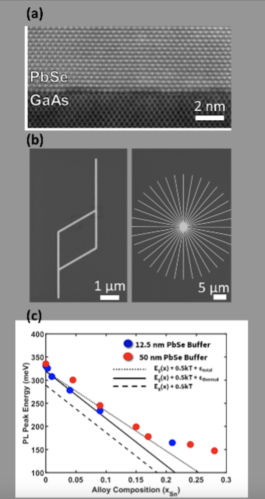
PbTe epitaxial films were first synthesized on GaAs in the 1980s for infrared devices,6 but the growth of IV-VI materials on III-V templates has since been revitalized to fabricate quantum devices. We refined the procedure to grow IV-VI semiconductors on III-V templates by molecular beam epitaxy and obtained samples with abrupt interfaces.7,8 Specifically, we showed that PbSe on GaAs formed a rather perfect incoherent interface as opposed to one that is riddled with misfit dislocations.9 In collaboration with Maksim Gomanko and Sergey Frolov, we have recently extended this work to PbSe selectively grown on patterned GaAs for nanowire devices. Mesoscopic studies of PbSe nanowire as spin qubit hosts are planned this year. Moving from PbSe to the alloy PbSnSe, we use photoluminescence (PL) from electron-hole recombination to track the bandgap narrowing. Bulk PbSnSe in the range of xSn = 0.2–0.4 is a topological crystalline insulator, the limit set by the stability of the rocksalt structure over the topologically trivial bandstructure in layered orthorhombic (GeS) structure. We find that thermal expansion mismatch is an important consideration for synthesis on GaAs that ends up keeping the gap wider than in the bulk by as much as 25% of the value at cryogenic temperatures. This increases the tin composition at which the film becomes topologically nontrivial. With the aim of achieving a larger bulk bandgap of the TCI phase, we are also quantifying the upper experimental limits of the rocksalt structure of PbSnSe under MBE growth conditions, recently showing novel transformation pathways to between the rocksalt and layered phase.10
References
1 G. Burkard, T.D. Ladd, A. Pan, J.M. Nichol, and J.R. Petta, “Semiconductor spin qubits,” Rev. Mod. Phys. 95(2), 025003 (2023).
2 M. Gomanko, E.J. de Jong, Y. Jiang, S.G. Schellingerhout, E. Bakkers, and S.M. Frolov, “Spin and Orbital Spectroscopy in the Absence of Coulomb Blockade in Lead Telluride Nanowire Quantum Dots,” SciPost Physics 13(4), 089 (2022).
3 G. Grabecki, J. Wróbel, T. Dietl, E. Papis, E. Kamińska, A. Piotrowska, A. Ratuszna, G. Springholz, and G. Bauer, “Ballistic transport in PbTe-based nanostructures,” Physica E: Low-Dimensional Systems and Nanostructures 20(3), 236–245 (2004).
4 J. Jung, S.G. Schellingerhout, M.F. Ritter, S.C. ten Kate, O.A.H. van der Molen, S. de Loijer, M.A. Verheijen, H. Riel, F. Nichele, and E.P.A.M. Bakkers, “Selective Area Growth of PbTe Nanowire Networks on InP,” Advanced Functional Materials 32(51), 2208974 (2022).
5 T.H. Hsieh, H. Lin, J. Liu, W. Duan, A. Bansil, and L. Fu, “Topological crystalline insulators in the SnTe material class,” Nature Communications 3, 982 (2012).
6 H. Clemens, H. Krenn, B. Tranta, P. Ofner, and G. Bauer, “Epitaxial growth of PbTe on (111)BaF2 and (100)GaAs,” Superlattices and Microstructures 4(4), 591–596 (1988).
7 B.B. Haidet, E.T. Hughes, and K. Mukherjee, “Nucleation control and interface structure of rocksalt PbSe on (001) zincblende III-V surfaces,” Phys. Rev. Materials 4(3), 033402 (2020).
8 B.B. Haidet, L. Nordin, A.J. Muhowski, K.D. Vallejo, E.T. Hughes, J. Meyer, P.J. Simmonds, D. Wasserman, and K. Mukherjee, “Interface structure and luminescence properties of epitaxial PbSe films on InAs(111)A,” Journal of Vacuum Science & Technology A 39(2), 023404 (2021).
9 B.B. Haidet, J. Meyer, P. Reddy, E.T. Hughes, and K. Mukherjee, “Versatile strain relief pathways in epitaxial films of (001)-oriented PbSe on III-V substrates,” Phys. Rev. Mater. 7(2), 024602 (2023).
10 P.D. Reddy, L. Nordin, L. Hughes, A.-K. Preidl, and K. Mukherjee, “Expanded stability of layered SnSe-PbSe alloys and evidence of displacive phase transformation from rocksalt in heteroepitaxial thin films,” (2023).