QF Faculty Member creates the first ever visualization of photoexcited charges traveling across the interface of two semiconductor materials
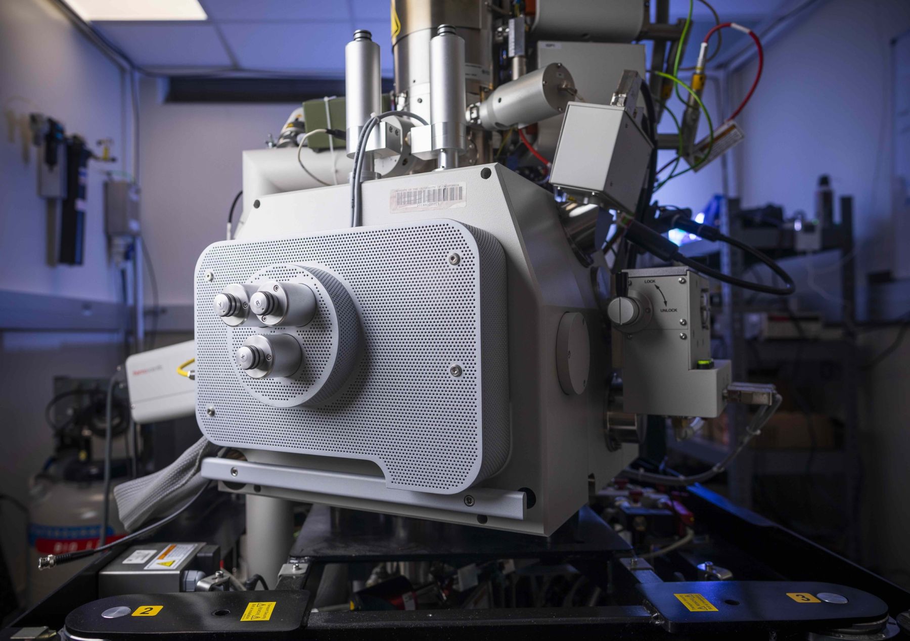
The ultrafast scanning electron microscope in the Bolin Liao lab
Excerpt from UCSB Current Science + Technology
UC Santa Barbara researchers have achieved the first-ever “movie” of electric charges traveling across the interface of two different semiconductor materials. Using scanning ultrafast electron (SUEM) techniques developed in the Bolin Liao lab, the research team has directly visualized the fleeting phenomenon for the first time.
“There are a lot of textbooks written about this process from semiconductor theory,” said Liao, an associate professor of mechanical engineering. “There are a lot of indirect measurements.” The ability to visualize how this process actually happens will allow semiconductor materials scientists to benchmark some of these theories and indirect measurements, he added.
The research is published in the Proceedings of the National Academy of Sciences.
‘Hot’ photocarriers
If you’ve ever used a solar cell, you’ve seen photocarriers in action: sunlight hits a semiconductor material, exciting electrons in the material, which move. This movement of electrons, and separation from their opposite-charged ‘holes,’ creates a current that can be harnessed to power electronic devices.
However, these photocarriers lose most of their energy within picoseconds (trillionths of a second) so that the energy that conventional photovoltaics harvests is but a fraction of the energy these carriers have in their “hot” state, before they cool down and release most of the excess energy as waste heat. While their hot state holds a lot of potential for things like energy efficiency, it also presents challenges within the semiconductor material, such as the heat that may affect device performance.
As a result, it’s important to get a good idea of how these hot carriers behave as they move through different semiconductor materials, and in particular how they move across the interface of two different materials — the heterojunction. In the realm of semiconductor materials, heterojunctions influence the movement of charge carriers for a variety of purposes, from the creation of lasers to photovoltaics to sensors to photocatalysis.
For the full article please see the link below